pre-processing


post-processing
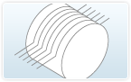
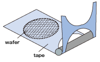
Protective tape lamination
Before applying the abrasive to the surface of the wafer, tape is affixed to protect the surface.

Grinding the under surface of the wafer
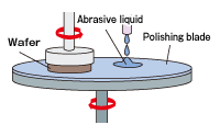
The under surface is ground to produce a lighter and thinner wafer.
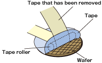
Removing the protective surface tape
After DAF is attached to the rear surface of the wafer, the wafer is fixed to the dicing frame.
After this, the protection tape is removed from the front surface in a continuous operation.
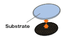
Substrates are detached from wafers without any stress.
No stress is given to wafers while substrates are separated.
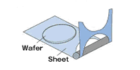
Die sheet lamination (Stacked IC)
Laminating die sheet on the backside of the wafer
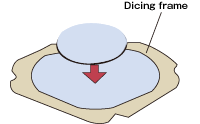

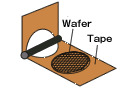
Wafer mount for dicing
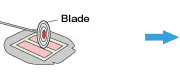
Dicing the wafer
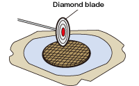
The wafer is cut and inspected, with only those wafers that are found to be good upon inspection being used for chips
UV irradiation

General Semiconductor Processing
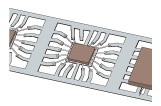
Wire Bonding
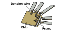
The chip and lead frame are connected using bonding wire (gold wire of approximately 25 μm thickness, etc.).
Packaging
The chip is inserted into a package made of ceramic, resin, etc.
Finished IC package
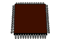
The semiconductor undergoes product and reliability inspections, and is finished after passing the inspections.
CSP (Chip Size Package) Process
Dry resist tape lamination
Pump formation
Dicing the wafer
The wafer is cut and inspected, with only those wafers that are found to be good upon inspection being used for chips
UV irradiation
Finished IC package
The semiconductor undergoes product and reliability inspections, and is finished after passing the inspections.
BGA Processing
Packaging
The chip is inserted into a package made of ceramic, resin, etc.
Substrate mounting for dicing
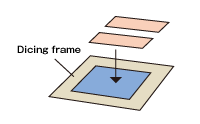
In order to prepare for dicing, tape is laminated onto frame and it is mounted.
Dicing
The package is cut and separated.
Placement in tray
CSP completion
After passing product and reliability inspections the CSP package is finished.

TAIKO® is a registered trademark of DISCO Corporation in Japan and other countries.

Equipment applicable to TAIKO® Process
Wafer Protective Tape Lamination Machines
Wafer Protective Tape Removal Machines
Film Resist Lamination Machines
Equipment applicable to Substrate (H-WSS) Processing (Attaching)
Equipment applicable to Substrate (H-WSS) Processing (Detaching)